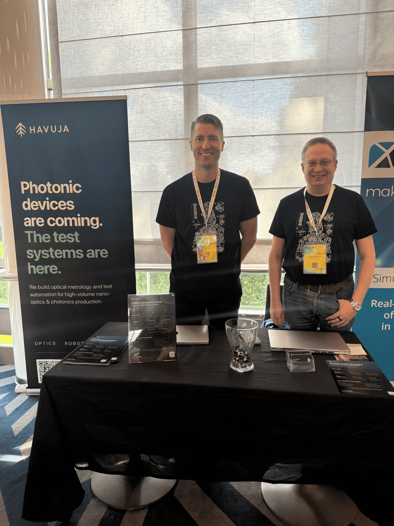

On 16–17 September our co-founders Pekka Laiho (CCO) and Kimmo Jokinen (CTO) were at High Tech Campus Eindhoven in the Netherlands for MicroLED Connect, AR/VR Connect and Optical I/O Connect.
The three co-located events are organized by TechBlick, MicroLED-Info and the MicroLED Industry Association. They bring together the companies building the next generation of displays and optics, from materials and equipment suppliers to device makers and the largest consumer-technology brands, with a program covering materials, equipment, manufacturing and device development.
This year’s edition launched a new track: Optical I/O Connect. It focuses on one of the biggest challenges in AI infrastructure, which is moving data between processors fast enough, far enough and at low enough power. Copper is efficient but short-reach. Optics reach further but bring trade-offs in power, cost and reliability. Talks covered new emitter and link architectures, integration with CMOS and silicon photonics processes, packaging and coupling losses, and how to manufacture all of this at scale.
The three tracks map closely to where Havuja works. MicroLED and AR/VR are about displays, waveguides and near-eye optics that have to be measured the way the user sees them. Optical I/O is about photonic links that have to be aligned, coupled and tested die by die. In all of them, the same question kept coming up: how do you test new optical devices at the speed and volume production demands?
With both a commercial and a technical co-founder on site, we could go from market conversations to deep technical discussions on optical metrology and test in the same meeting. Thank you to everyone who met with us in Eindhoven.
If testing and metrology are a challenge as you move toward production, we’d like to hear about it. [Talk to an engineer →]
Learn more: